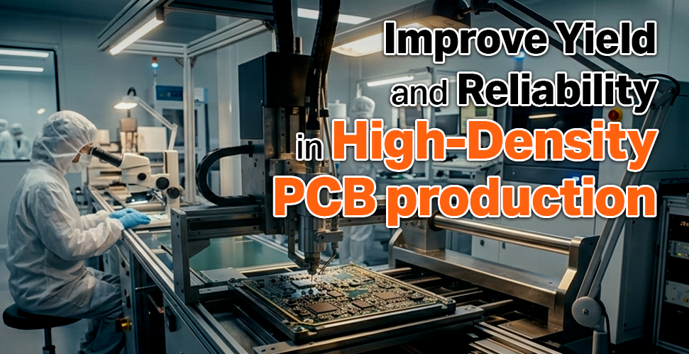
As electronics move toward extreme miniaturization, the margin for error in PCB manufacturing has effectively vanished. For those operating in the high-density (HDI) and multi-layer space, a 1% drop in yield isn't just a waste of materials, but a direct hit to your bottom line and your reputation for reliability.
|
|
|
|
|
|---|
|
|
| The Precision Paradox: As line spacing and via sizes shrink, traditional etching and plating methods are hitting a "yield wall," leading to higher scrap rates and electrical failures. |
|
|
|
|
|---|
|
|
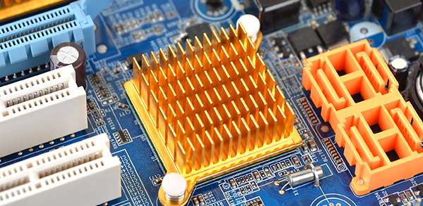
| Thermal Management Stress: High-performance boards for AI and 5G demand superior thermal dissipation. Without advanced substrate materials and precise copper distribution, reliability is compromised. |
|
|
|
|
|---|
|
|
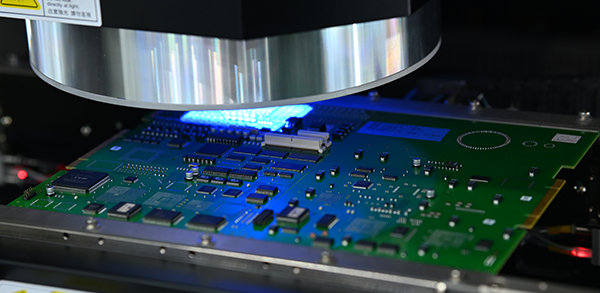
| Assembly Complexity: Placing 008004 components or ultra-fine pitch BGAs requires a level of placement accuracy and solder paste inspection (SPI) that legacy machines simply cannot achieve. |
|
|
|
|
|---|
|
|
NEPCON Thailand 2026 is your platform to break through these technical bottlenecks and achieve the "Zero-Defect" goal in high-density production with solutions from suppliers of global brands. For example, the latest Laser Direct Imaging (LDI) and high-resolution AOI, jet fluxing and high-speed solder paste printing technologies that ensure consistent volume and placement, the next generation of ICT (In-Circuit Testing) and Flying Probe testers designed to validate reliability under extreme conditions, and many more to help you turn challenging high-density specs into routine, high-yield production from the outset. |
|
|
|
|
|---|
|
|
| |
|