Email not displaying correctly? View it in your browser.
eNewsletter 20
The race for faster chips has hit a physical wall. As transistors become too small to shrink further without massive costs, the industry has shifted its focus. The next generation of performance won't come from the chip alone, but from how it is packaged. 

Current Challenges in the Semiconductor Landscape
  • Higher processing power in smaller AI and 5G devices cause intense "hotspots" that traditional packaging cannot cool, leading to thermal throttling and hardware failure.
  • The move toward "Chiplets" and heterogeneous integration massively increase in interconnect complexity, requiring bonding precision and cleanliness that exceeds standard cleanroom capabilities.
  • More complex 2.5D and 3D packaging structures can cause catastrophic yield loss. A single defect during the final packaging stage now means throwing away expensive, high-functioning silicon.
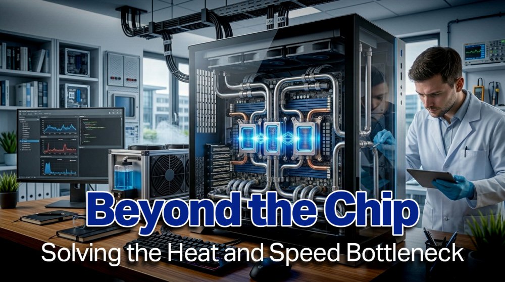
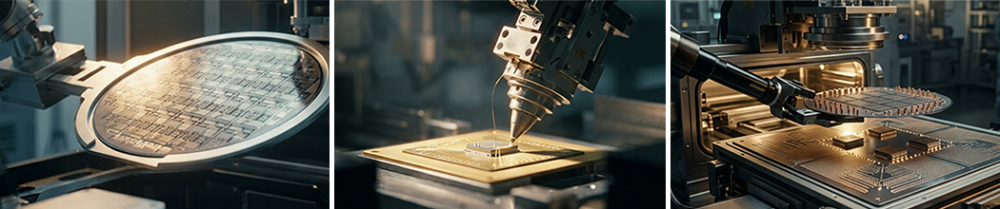
Don't let legacy assembly methods limit your production yield. At NEPCON Thailand, you can source the specific technologies from global brands required to handle the complexity of modern semiconductor back-end, including High-Precision Bonding & Die Attach, Wafer-Level & Panel-Level Processing (WLP/PLP) with the latest lithography and plating equipment designed to increase throughput, and AI-Driven Automated Testing (ATE) that can detect sub-micron defects in complex 3D structures, ensuring maximum reliability before your product leaves the factory floor.  Join us in upgrading your factory to handle high-value, advanced chip packaging and become part of a world-class supply chain at this event.